
I finally got a chance today to try my planned board modification to fix the design flaw I foolishly put on my board. Just a couple cuts with the dremel to isolate the section of the ground plane that connects the LEDS:
Two cuts to the board and it suddenly becomes useful!
Testing with the continuity checker, it looks like I have managed to remove that section from the ground plane, so now I can instead hook it to Vcc. Not ideal, but it should work. I do have just one more flaw to fix in the board before I can use it. As far as I can tell, this is not my fault, but a manufacturing defect that hit all 3 of my boards exactly the same:
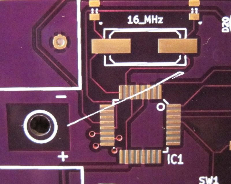
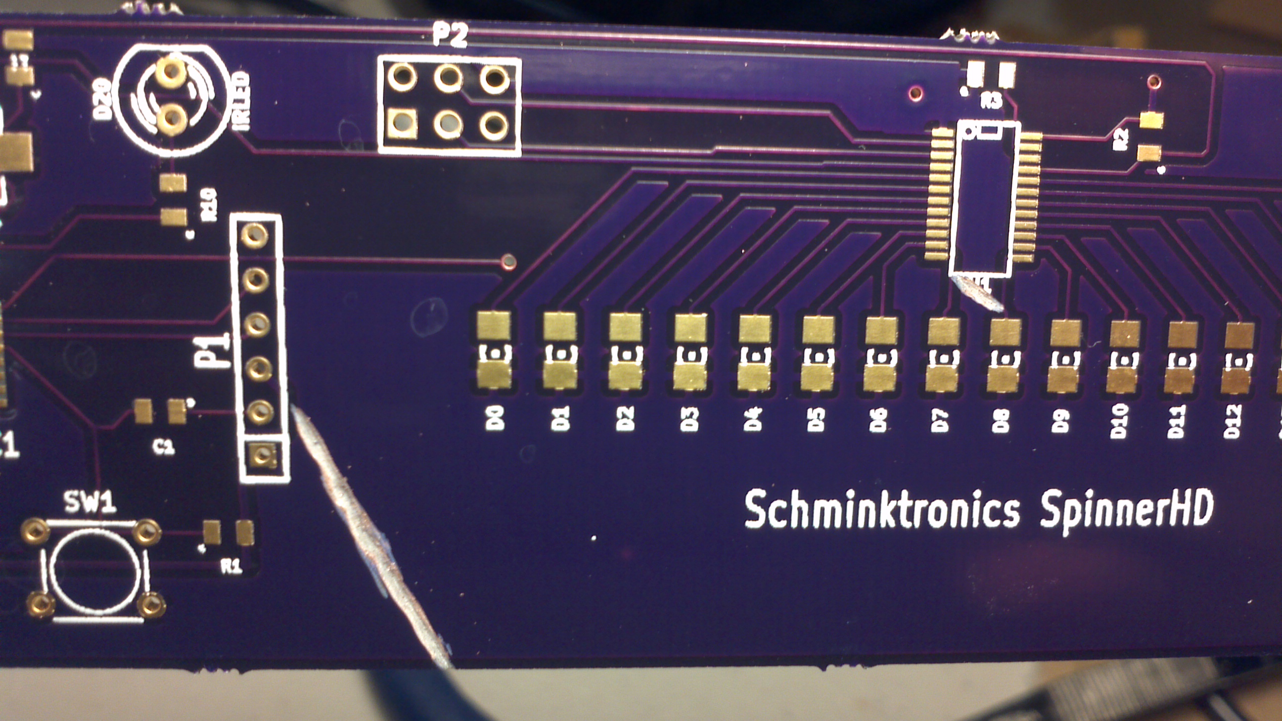
Silkscreen layer got printed on top of my pads!
For some reason, the silkscreen layer got printed on top of my pads! I looked at my gerbers for the silkscreen and that line isn’t there. It almost looks like the machine just malfunctioned and dribbled out while it moved across the board except that the exact same flaw appears on all three of my boards. Even if it was in my gerbers, the printer is supposed to skip printing anything that crosses a pad. In fact–in the gerbers, there’s a full outline for that chip that didn’t get printed before it went across the pads. Something really went wrong to get it there.
The board might work without me doing anything, but to be safe, I’ve got to clean that off before I spend time trying to securely solder the processor on there. Hopefully that peels off easily…